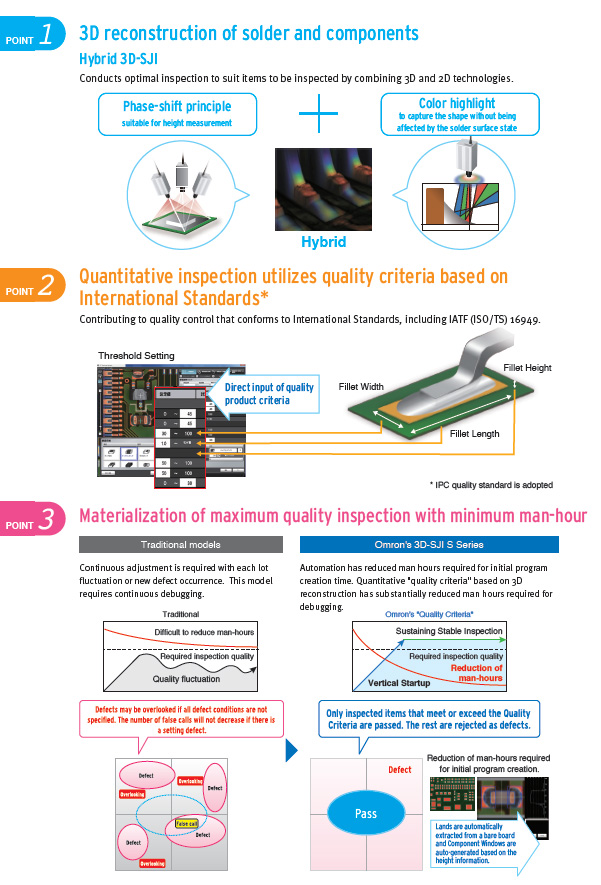
Materializes quantitative inspection of solder joint and implementation, while minimizing risks of overlooking unknown defects by the quality product criteria inspection based on the standards, contributing to vertical startup of inspection.
2026/03 停產商品
VT-S530
PCB Inspection System
Omron's 3D-SJI (Solder Joint Inspection) Ensuring High-quality Products in an Efficient Manufacturing Environment
此頁記載內容是在依據停產前商品型錄內刊載的資訊,包括商品的特點 /價格 /對應規格 /選購品等,可能會和現狀有所出入。請在選購前再次確認系統的適用性及安全性。
更新日期 2019年4月15日
Omron's 3D-SJI (Solder Joint Inspection)
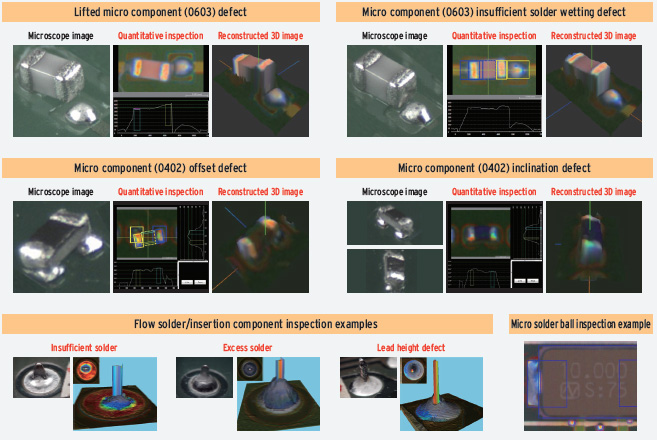
Example Defects
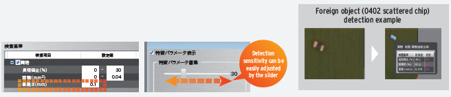
Whole PCB surface inspection
Detecting foreign objects accurately is achieved through combining 3D (height) and 2D (area) measurements on the entire PCB surface. (Lands without solder can be excluded from the inspection)
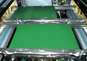
High productivity inspection
High production throughput supported through dual lane.
Dual lane operation using various PCBs is possible, due to its handling capability up to the PCB size of 510 (W) x 330 (D) mm.
更新日期 2019年4月15日
© Copyright OMRON Corporation 1996 - 2023. All Rights Reserved.